
Vacuum Boosters for Semiconductor Manufacturing
High levels of vacuum are required to maintain operating conditions and perform the various manufacturing steps for precise production of semiconductor wafers to be incorporated into electronic components such as computer processors. To reduce costs while achieving high performance, a vacuum booster can be implemented into the vacuum system.
Deposition is one of the most important steps for semiconductor manufacturing. In this step, layers of dielectric and conductive silicon dioxide and silicon nitride are laid onto the silicon wafer. Along with a top layer of photoresist, these layers are added to trace a path for which the etching agent can follow to create the proper troughs within the silicon. Depending on the pattern, the semiconductive properties of the wafer are amplified, increasing its performance in electronic equipment. There are many different variations of deposition to achieve a similar effect with different advantages and disadvantages, such as physical vapor deposition (PVD), plasma enhanced chemical vapor deposition (PECVD), sub-atmospheric chemical vapor deposition (SACVD), low pressure chemical vapor deposition (LPCVD), atomic layer deposition (ALD), high density plasma chemical vapor deposition (HDPCVD) and many more. A significant number of these deposition techniques are required or recommended to be done under high vacuum pressure, which helps to vaporize the material that is to be deposited. The material is vaporized to achieve more uniform and precise thicknesses of deposited layers to reduce error when etching. The vacuum has an added effect of keeping the surroundings of the silicon wafer clean and free from suspended particulate matter which may damage the silicon wafer or hinder the entire process.
After the layers are deposited, the next step is photolithography, where a beam is emitted onto the photoresist, which is a polymer that changes solubility depending on radiation that is emitted onto it. The electromagnetic radiation of the beam is used to cut into the photoresist, drawing the desired pattern to be etched into the silicon. The step after photolithography is to strip (etch) and clean the wafer. The wafer is cleaned while layers are selectively removed. There are many different methods of etching as well, but the main idea is that the deposited layers form a barrier against the etchant where the silicon should not be etched. The deposited layers also form a guide for the etchant on the particular patterns that should be etched within the silicon along with the patterned photoresist, all while the wafer is being cleaned so that no sharp fragments are etched off and scratch or cut the silicon. This is done under vacuum as well, at an approximate 1 mbar of atmosphere, and the wafer is subsequently washed with deionized, degassed, and distilled water to get rid of any smaller impurities that may be on the wafer.
Once the wafer is etched and cleaned, the silicon wafer is doped in the etched regions. Ions are implanted into the troughs using different methods such as beamline, end station, or ion source. The doping of the semiconductor allows it to attain the electrical properties desired of the semiconductive material for calculating, computing, and simple logic applications. To guarantee an absolutely clean environment so that a uniform layer of ions are implanted throughout the entirety of the etched pattern, an atmosphere of 10-8 mbar is employed. Once the ion implantation is completed, metal links are laid between transistors to create the complex yet easily recognizable semiconductor water pattern.
As this process occurs, the wafer must be transported between the evacuated stations where the deposition, photolithography, etching, cleaning, and ion implantation takes place. The wafers must be handled with care, but they also must not be exposed to atmospheric impurities such as the aforementioned suspended particulate matter. As such is the case in automated semiconductor mass-manufacturing, wafer handling and conveying are all done in vacuum conditions as well. This guarantees a precise, clean, high-quality semiconductor wafer.
Once manufacturing is complete, the wafer is kept under vacuum as it is inspected and measured. If any impurities were to come in contact, the semiconductor will most likely fail in operation, as semiconductor technology has miniaturized to the atomic scale thanks in full to the rapidly advancing research in technology that has been done in recent decades.
The Impact of the Semiconductor Industry
The semiconductor wafers are widely used in communications, national defense, computing, transportation, energy, healthcare, commercial electronics, automotive and aviation vehicles, and countless more applications. Semiconductive material is increasingly prevalent in modern society, projected to become a trillion-dollar industry by 2030. Everywhere one can currently look, a semiconductor will be within the field of view.
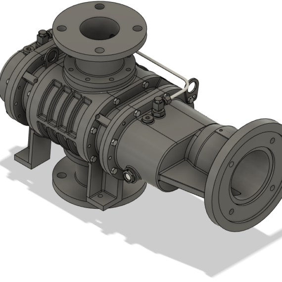
Advantages of NES Company In.c NB Series Vacuum Boosters
Typically, a turbopump or cryopump are used for the finer vacuum levels required in semiconductor manufacturing, with a dry roughing vacuum pump such as a dry screw vacuum pump. Using a vacuum booster with the dry screw vacuum pump will boost pumping speeds and allow for a higher achievable vacuum pressure at a lower power requirement, increasing the efficiency of the vacuum system. The system will rough quicker at a higher level of vacuum, significantly reducing strain on the main vacuum pump, whether it be a cryopump or turbomolecular pump.
NES Company Inc. is proud to offer the NB Series two-lobe vacuum booster with five-point mechanical seal and double oil tanks for more stable and fast lubrication and operation. Including an internal corrosion-resistant coating and nitrogen gas barrier to prevent oil contamination and reduce oil consumption, NES Company Inc. provides various optional seals and coatings for the perfect booster in any system and application.