
Semiconductor Manufacturing Rotary Vane Vacuum Pumps & Compressors
Vacuum technology is prevalent in the modern semiconductor manufacturing process from beginning to end. The artificially induced vacuum conditions create both the environment and technique required for precise and clean production.
Semiconductive material was first discovered as useful electronic material in 1874 with the invention of the AC-DC converter, or rectifier. After this, a series of inventions came in rapid progression, reigning in the era of transistors. These transistors switched on and off, and compiling binary data through a massive number of moving transistors became the new way to collect and store information. These transistors were built by the thousands on singular chips, organized in circuit boards known now as semiconductors. As computers were invented, developed, and streamlined, the need for smaller semiconductors became clear. New methods of semiconductor manufacturing were developed, and the semiconductors became smaller and smaller. The result of this was that more information could be stored, collected, and transferred at an accelerating rate. The issue with this is that the smaller a semiconductor is, the more difficult it is to manufacture. Strict tolerancing must be enforced, meaning more expensive equipment and longer process time. The environment must be entirely clean, and the semiconductor itself must be cleaned and rinsed so that impurities do not affect the tiny semiconductors, as even the smallest scratch will irreversibly damage the semiconductor and hinder its performance or render it useless. Even the cleaners used to clean the semiconductors are specially treated and cleaned. Especially in recent years, leaps and bounds in technique and technology have been made in order to meet the harsh requirements placed on the production of semiconductors.
Semiconductors make use of quartz crystals due to the physical properties that they naturally exhibit. Depending on the cut and size of these crystals, they will begin to vibrate at specific frequencies that can be imposed via electricity. When mechanical stress is applied to these crystals, they begin to oscillate and store electrical charge in a phenomenon known as the piezoelectric effect. This phenomenon is used to the advantage of certain electronic devices, but especially so in the semiconductor, where binary data is stored through the determination of electric charge being charged or not charged per crystal unit. For this reason, the precise formulation and growth of quartz crystals is important to semiconductor manufacturing and entails a specialized procedure.
To grow quartz crystals of correct sizing and cut, naturally formed quartz crystals are ground and diluted in a solvent, typically water. Naturally occurring crystals contain impurities and defects as they develop in an environment covered in dirt and dust. Once the solution is made, it is placed in a vacuum chamber. The pressure within the chamber is lowered to a controlled degree, which influences the boiling point of the solvent. The solvent evaporates at a rate dependent on the vacuum level and temperature in the chamber, separating the impurities as the solute crystal begins to reform. By the time that the crystals have reformed, the impurities have been removed by the solvent, which has now completely evaporated.
Once the crystals have been formed and used to construct the semiconductor wafer, layers of pad oxide, nitride, anti-reflective coating, photoresist, and glass are placed on top of the wafer. Photoresists are polymers that are soluble when exposed to ultraviolet light. The photoresist is manipulated to shape a pattern on top of the substrate layers below it. Once the shape is formed, it is used as a stencil of sorts, as the carbon hard mask is etched from the top so that every part of it is removed except for that under the photoresist. The rest of the photoresist is stripped off, as well as the anti-reflective coating. The rest of the wafer and layers are etched according to the new shape of the hard mask, and the latter is removed, resulting in a finished semiconductor wafer. These wafers are used in various electronic devices, such as solar cells and computer central processing units.
Etching allows for complex structures to be constructed on miniature scales. Wet etching uses hot liquid etchants to cut into the material on the wafer. Wet etching is extremely versatile and applicable to many different substrates. Dry etching, or plasma etching, is the use of plasma etchants in a pressure-controlled atmosphere to cut into the wafer. Dry etching is significantly more controlled and precise with the cutting, and is useful for more complex circuitry.

Applications of NES Vacuum Pumps
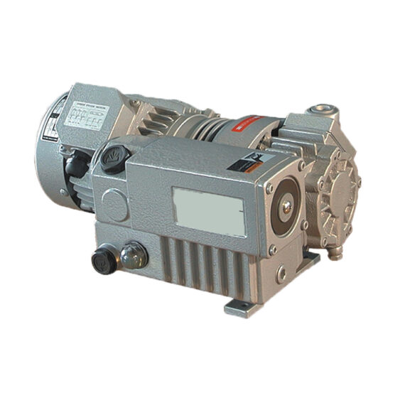
Oil-circulated rotary vane vacuum pumps are widely used as forepumps (backing pumps) for plasma etching and crystal growth. Depending on the etchant, plasma etching procedures may require less than Torr of atmospheric pressure within the etching chamber. An ultra-high level vacuum pump such as a turbomolecular pump, cryopump, or diffusion pump are required for this process. However, using the singular ultra-high vacuum pump to lower the pressure from 760 Torr to a fraction of a Torr is highly discouraged. When an ultrahigh vacuum pump with complex design is operated for long periods of time from atmospheric pressure to near complete vacuum, much maintenance and repair is to be expected. Using a simpler pump that is able to raise the vacuum pressure benefits the ultrahigh vacuum pump by allowing it to begin evacuation at an intermediate step, translating to less work for the complex pump with many working parts.
Similarly, crystal growth takes place at a range of different pressure levels depending on the composition of the quartz; BiS2 crystal growth is performed at a recommended Torr. While this does not warrant an ultrahigh vacuum pump, a high vacuum pump is required to reach this level of vacuum and a backing pump is still extremely useful in this situation.
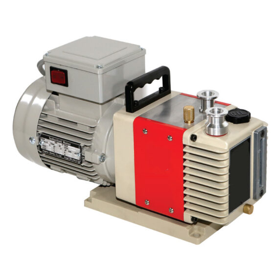
Advantages of NES Vacuum Pumps
The advantages of using the NES Company Inc. NRV Series oil-flooded rotary vane vacuum pump models are cost, simplicity, and versatility. Using a different vacuum pump, like a dry screw or dry claw vacuum pump, as a backing pump for these applications will cost nowhere near as low as the rotary vane vacuum pump. The rotary vane pump features a simple design with few moving parts, allowing for simpler maintenance and repair. This pump is constructed with a robust design and the oil within the pump lubricates the vanes, seals the space in between the vanes and chamber, and protects the inner parts from mildly corrosive process gasses. This translates to higher vacuum level and longer service life.